
Home
/
Surenoo Graphic OLED Module 1.3" 12864 128*64 128X64 Graphic LCD Module Display Screen Panel PM-OLED 6800/8080 8-Bit Parallel 4-Wire Serial SPI IIC I2C SH1106 Controller SOG12864D_M130 P130
Surenoo Graphic OLED Module 1.3" 12864 128*64 128X64 Graphic LCD Module Display Screen Panel PM-OLED 6800/8080 8-Bit Parallel 4-Wire Serial SPI IIC I2C SH1106 Controller SOG12864D_M130 P130
WISHLIST
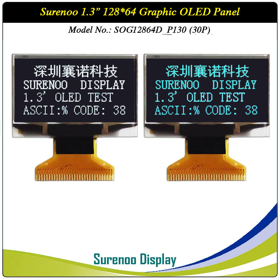
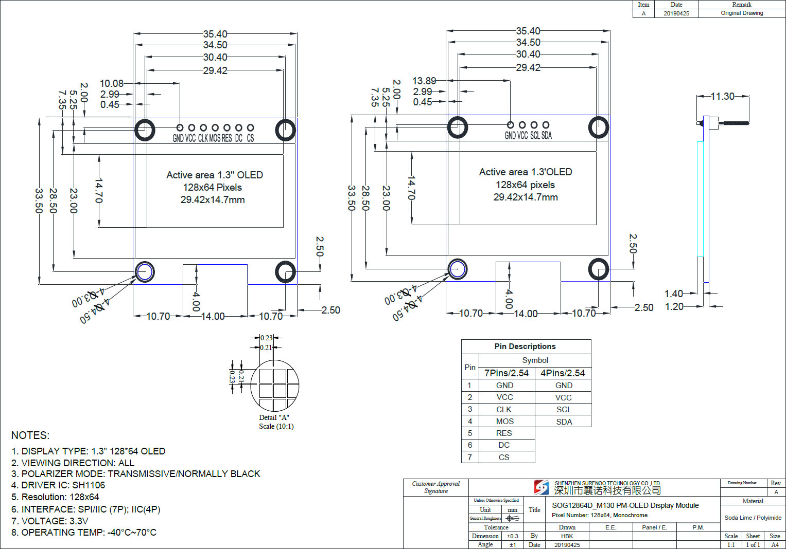
Display Size: 1.3"
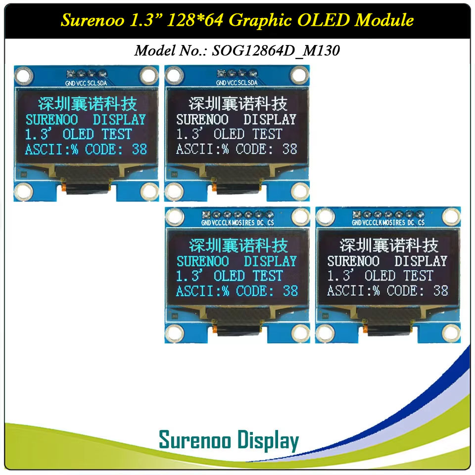
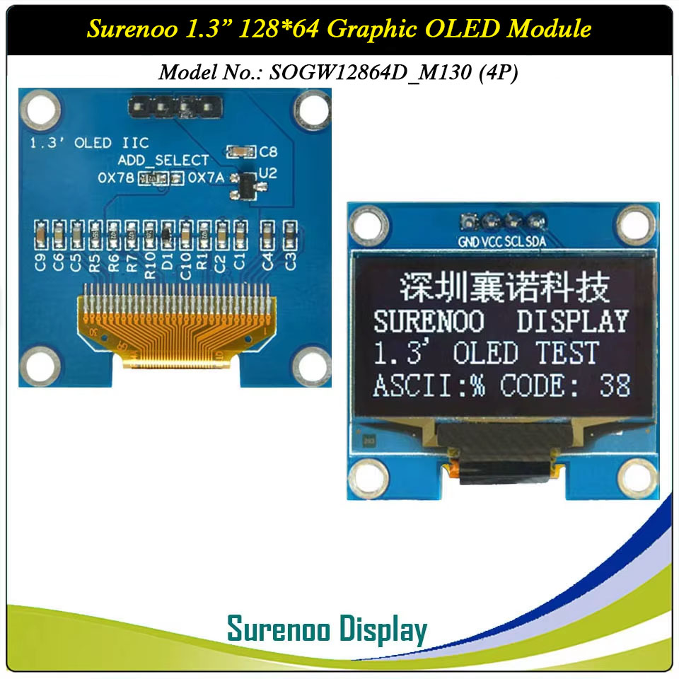
Model No.: SOG12864D_M130
Display Format: 128*64 Dots
Outline: 35.40X33.50MM
Controller: SH1106 or Equal
Model No.: SOG12864D_M130
Display Format: 128*64 Dots
Outline: 35.40X33.50MM
Controller: SH1106 or Equal
47 sold
Quantity
-
Detail
- Overview
- Specification
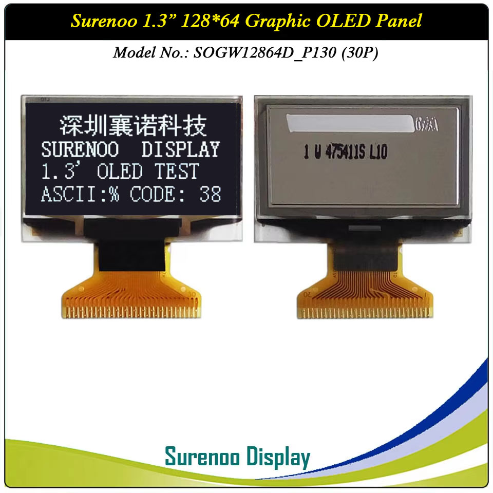
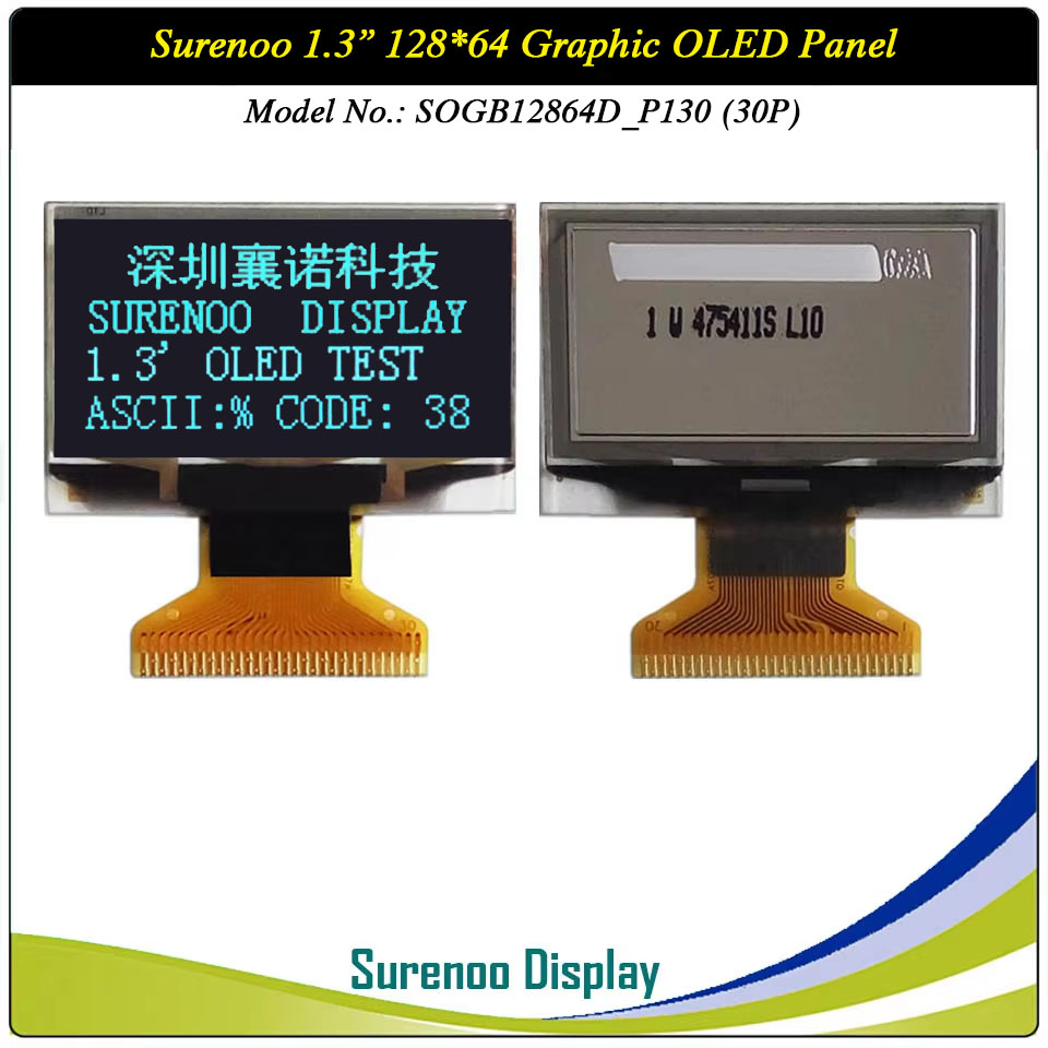
Gross Weight 0.020Kg Manufacturer Surenoo Display Type Graphic OLED Module / Graphic OLED Panel Continuity Supply More than 10 years Part No. SOG12864D_M130 Diagonal Size (Visual Area) 1.3" Display Format 128*64 Dots Interface 7P: Serial SPI / IIC; 4P: IIC IC or Equivalent SH1106 or Equal Voltage(Type) 3.3V Outline Dimension 35.40(W)x33.50(H)x2.60(T)mm Visual Area 31.42x16.70mm Active Area 29.42x14.70mm Dots Size 0.21x0.21mm Dots Pitch 0.23x0.23mm Display Type PM-OLED Panel Colors Code White(SOGW) / Blue(SOGB) IC Package COG Viewing Direction Full Viewing Angle Operating Temperature-40℃~70℃Storage Temperature-40℃~80℃- Outline Drawing
2. SOG12864D_P130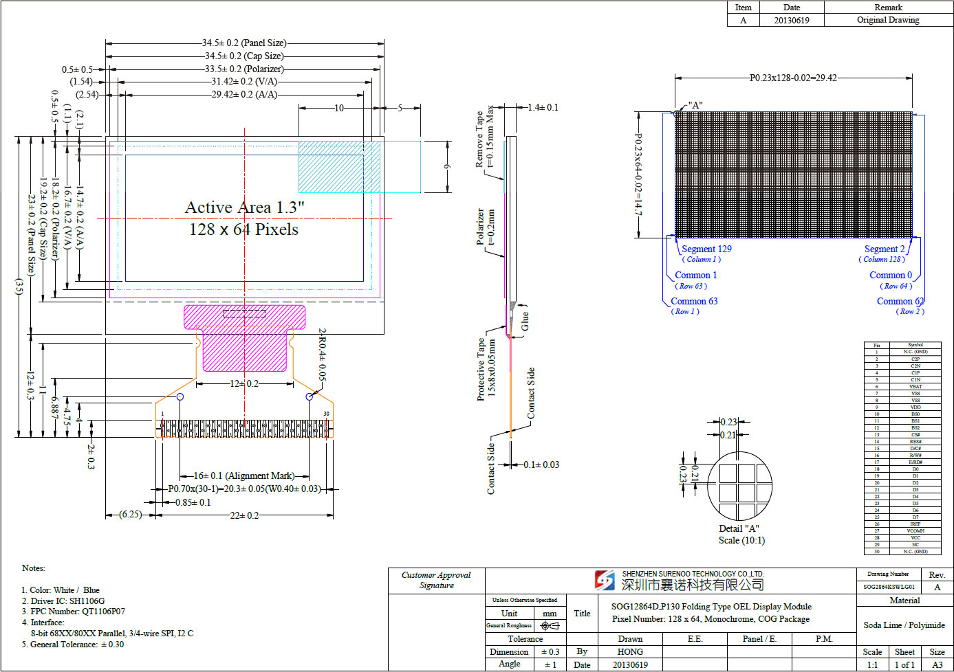
- Interface
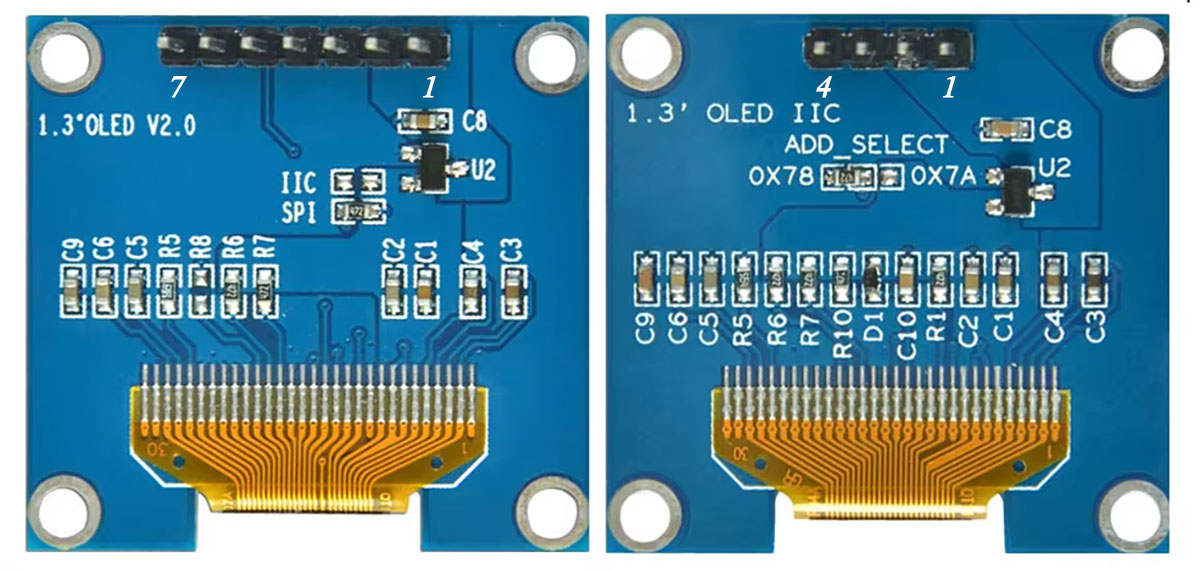
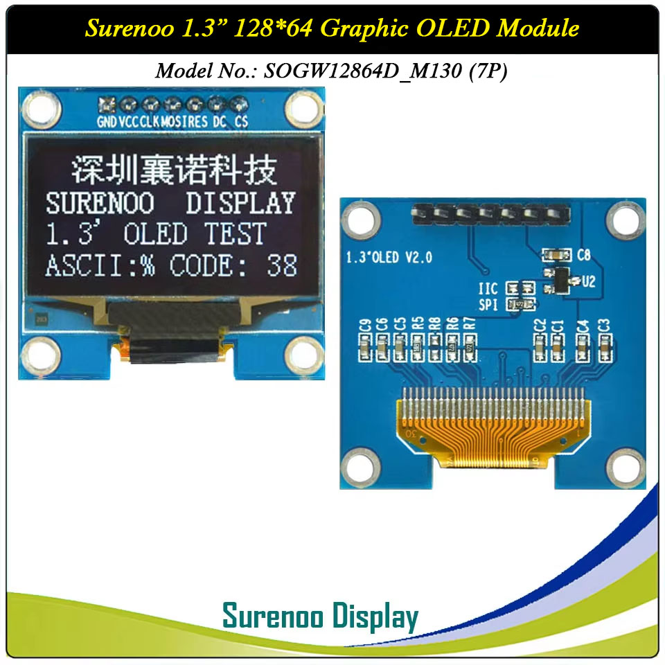
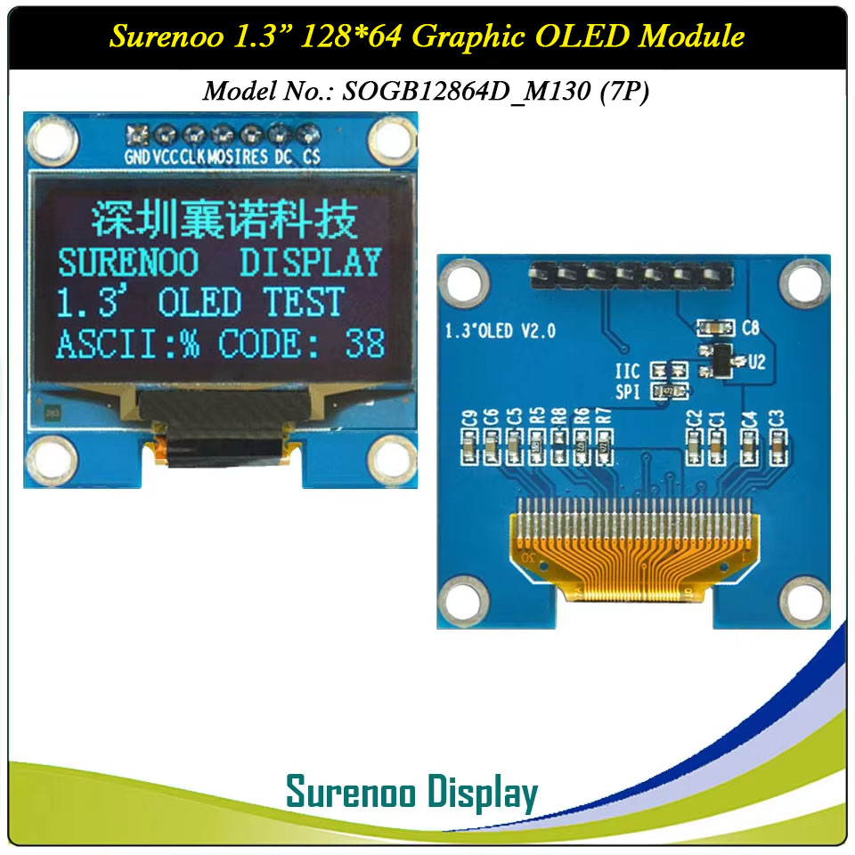
1.1 SOG12864D_M130 (7Pins)Pin No. Symbol Description 1 GND (0V) Ground 0V 2 VCC (3.3V) Power Supply for logic 3 CLK (H/L) The serial clock input SCL 4 MOS (H/L) The serial data input SDA 5 RES Reset signal, Active LOW 6 SPI: D/C IIC: NC SPI: H: Data L: Command IIC: No Connection 7 SPI: CS IIC: NC SPI: Chip Selection, Active LOW IIC: No Connection
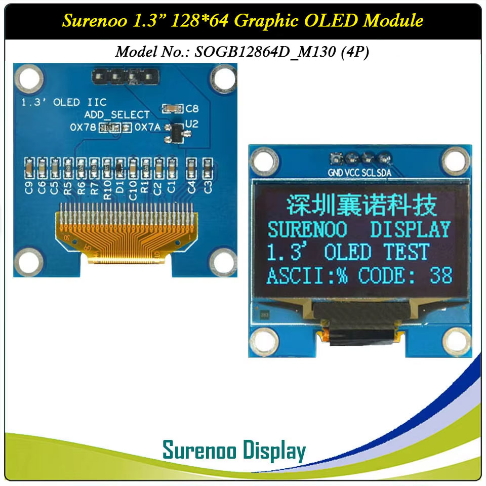
1.2 SOG12864D_M130 (4Pins)Pin No. Symbol Description 1 GND (0V) Ground 0V 2 VCC (3.3V) Power Supply for logic 3 SCL (H/L) The serial clock input SCL 4 SDA (H/L) The serial data input SDA
2. SOG12864D_P130 (30P/0.7)
Pin No. Symbol Type Description Power Supply 9 VDD P Power Supply for Logic Circuit
This is a voltage supply pin. It must be connected to external source.8 VSS P Ground of OEL System
This is a ground pin. It also acts as a reference for the logic pins, the OEL driving voltages, and the analog circuits. It must be connected to external ground.28 VCC P Power Supply for OEL Panel
This is the most positive voltage supply pin of the chip. It must be supplied externally.29 VLSS P Ground of Analog Circuit
This is an analog ground pin. It should be connected to VSS externally.Driver 26 IREF I Current Reference for Brightness Adjustment
This pin is segment current reference pin. A resistor should be connected between this pin and VSS. Set the current at 12.5uA.27 VCOMH O Voltage Output High Level for COM Signal
This pin is the input pin for the voltage output high level for COM signals. It can be supplied externally or internally. When VCOMH is generated internally, a capacitor should be connected between this pin and VSSDS/DC Convert 6 VBAT P Power Supply for DC/DC Converter Circuit
This is the power supply pin for the internal buffer of the DC/DC voltage converter.It must be connected to external source when the converter is used. It should be connected to VDD when the converter is not used.4 / 5
2 / 3C1P / C1N
C2P / C2NI Positive Terminal of the Flying Inverting CapacitorNegative Terminal of the Flying Boost CapacitorThe charge-pump capacitors are required between the terminals. They must be floated when the converter is not used.Interface 10
11
12BS0
BS1
BS2I Communicating Protocol SelectThese pins are MCU interface selection input. See the following table:BS0 BS1 BS2 I2C 0 1 0 3-wire SPI 1 0 0 4-wire SPI 0 0 0 8-bit 68XX Parallel 0 0 1 8-bit 80XX Parallel 0 1 1 14 RES# I Power Reset for Controlle and Driver
This pin is reset signal input. When the pin is low, initialization of the chip is executed.13 CS# I Chip Select
This pin is the chip select input. The chip is enabled for MCU communication only when CS# is pulled low.15 D/C# I Data/Command Control
This pin is Data/Command control pin.
When the pin is pulled high, the input at D7~D0 will be interpreted as display data. When the pin is pulled low, the input at D7~D0 will be transferred to the command register.When the pin is pulled high and serial interface mode is selected, the data at SDIN will be interpreted as data. When it is pulled low, the data at SDIN will be transferred to the command register.
In I2C mode, this pin acts as SA0 for slave address selection.For detail relationship to MCU interface signals, please refer to the Timing Characteristics Diagrams.17 E/RD# I Read/Write Enable or Read
This pin is MCU interface input.
When interfacing to a 68XX-series microprocessor, this pin will be used as the Enable (E) signal. Read/write operation is initiated when this pin is pulled high and the CS# is pulled low.When connecting to an 80XX-microprocessor, this pin receives the Read (RD#) signal. Data read operation is initiated when this pin is pulled low and CS# is pulled low.When serial or I2C mode is selected, this pin must be connected to VSS.16 R/W# I Read/Write Select or Write
This pin is MCU interface input.
When interfacing to a 68XX-series microprocessor, this pin will be used as Read/Write (R/W#) selection input. Pull this pin to “High" for read mode and pull it to “low" for write mode.When 80XX interface mode is selected, this pin will be the Write (WR#) input. Data write operation is initiated when this pin is pulled low and the CS# is pulled low.When serial or I2C mode is selected, this pin must be connected to VSS.18~25 D0-D7 I/O Host Data Input/Output Bus
These pins are 8-bit bi-directional data bus to be connected to the microprocessor’s data bus.
When serial mode is selected, D1 will be the serial data input SDIN and D0 will be the serial clock input SCLK.
When I2C mode is selected, D2 & D1 should be tired together and serve as SDAout & SDAin in application and D0 is the serial clock input SCL.Unused pins must be connected to VSS except for D2 in serial mode.Reserve 7 NC - Reserved Pin
The NC pin between function pins are reserved for compatible and flexible design.1, 30 NC (GND) - Reserved Pin (Supporting Pin)
The supporting pins can reduce the influences from stresses on the function pins. These pins must be connected to external ground.
-
Customer ReviewsNo comments