Home
/
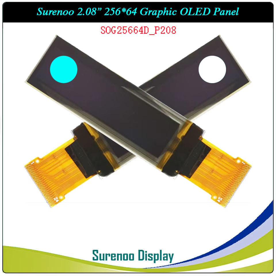
Surenoo Graphic OLED Module 2.08" 25664 256*64 256X64 Graphic LCD Module Display Screen Panel PM-OLED 6800/8080 8-Bit Parallel 3-/4- Wire Serial SPI I2C IIC SH1122 Controller SOG25664D_P208
Surenoo Graphic OLED Module 2.08" 25664 256*64 256X64 Graphic LCD Module Display Screen Panel PM-OLED 6800/8080 8-Bit Parallel 3-/4- Wire Serial SPI I2C IIC SH1122 Controller SOG25664D_P208
WISHLIST
Display Size: 2.08"
Model No.: SOG25664D_P208
Display Format: 256*64 Dots
Outline: 60.50X19.00MM
Controller: SH1122 or Equal
Model No.: SOG25664D_P208
Display Format: 256*64 Dots
Outline: 60.50X19.00MM
Controller: SH1122 or Equal
8 sold
Quantity
-
Detail
- Overview
It's easily controlled by MCU such as 8051, PIC, AVR, ARDUINO, ARM and Raspberry Pi. It can be used in any embedded systems, industrial device, security, medical and hand-held equipment.
- Specification
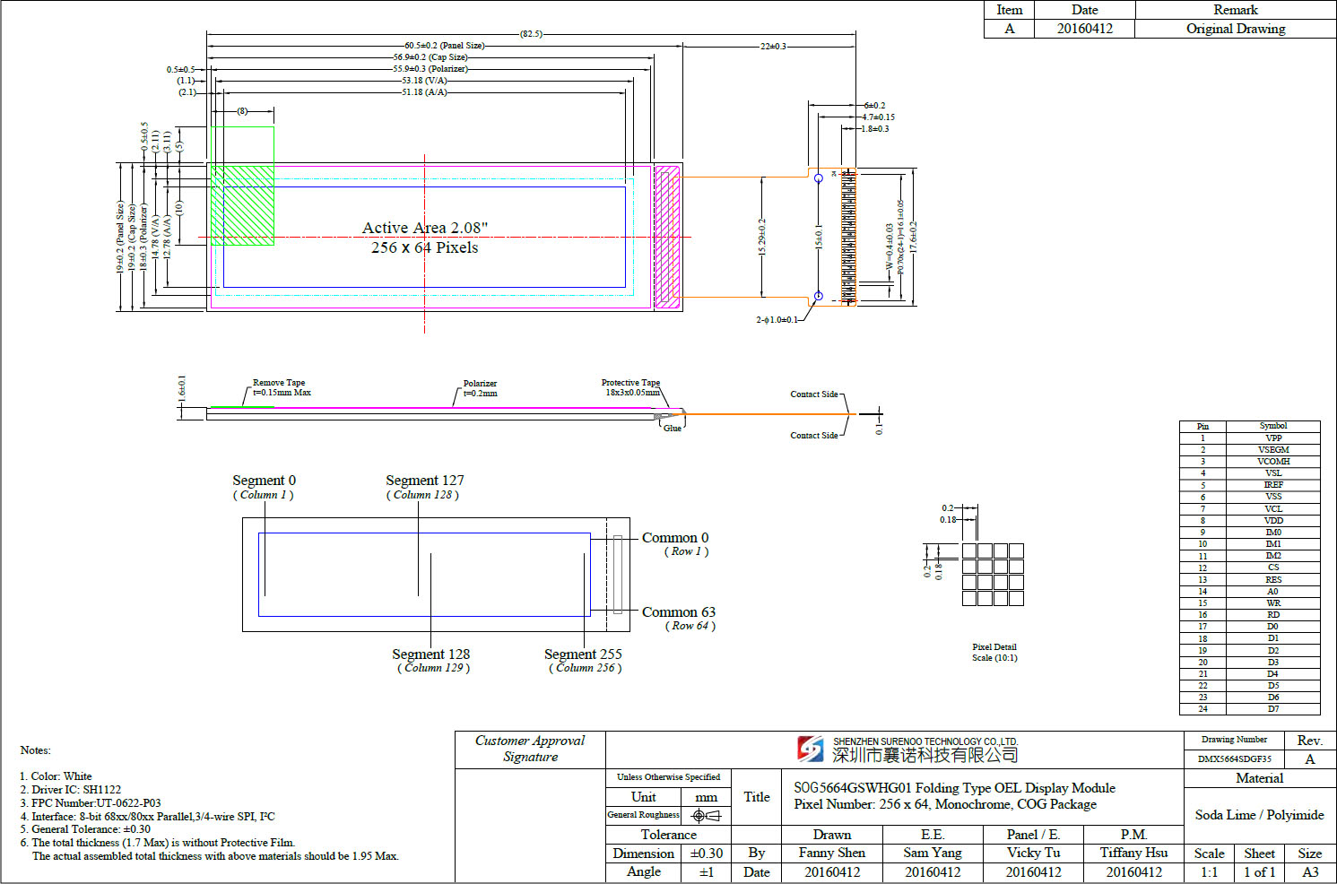
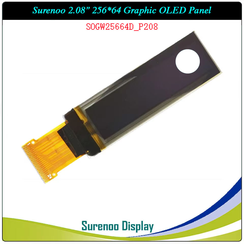
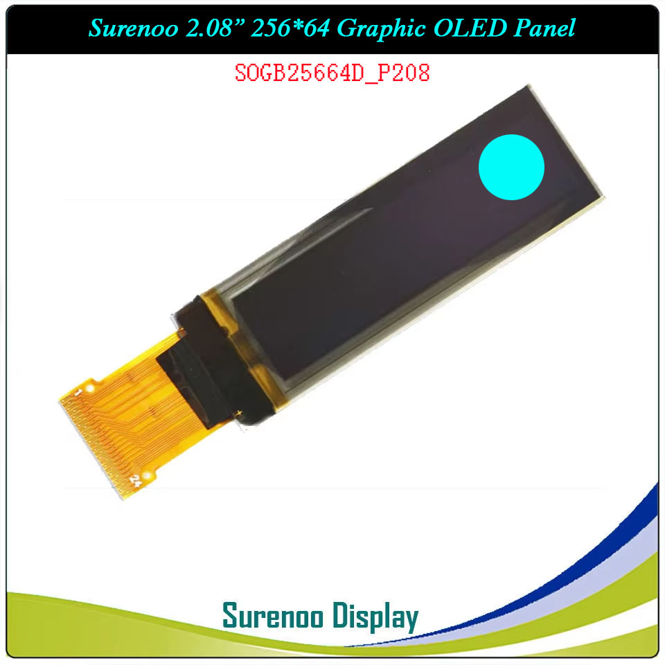
Gross Weight 0.060Kg Manufacturer Surenoo Display Type Graphic OLED Module / Graphic OLED Panel Continuity Supply More than 10 years Part No. SOG25664D Diagonal Size (Visual Area) 2.08" Display Format 256*64 Dots Interface SPI/IIC IC or Equivalent SH1122 or Equal Voltage(Type) 3.3V Outline Dimension 60.50(W)x19.00(H)x1.60(T)mm Visual Area 53.18x14.78mm Active Area 51.18x12.78mm Dots Size 0.20x0.20mm Dots Pitch 0.18x0.18mm Display Type PM-OLED Panel Colors Code SOGW(White) / Green(SOGG) / Blue(SOGB) IC Package COF Viewing Direction Full Viewing Angle Operating Temperature-40℃~70℃Storage Temperature-40℃~80℃- Outline Drawing (OLED Panel: SOG25664D_P208)

- Interface <OLED Panel: SOG25664D_P208 (24Pin/0.5)>
Please download the datasheet to get the detailed Pin descriptionPin No. Symbol Type Description Power Supply 1 VPP P Power Supplly for OEL Panel
These are the most positive voltage supply pin of the chip. They must be connected to external source.6 VSS P Ground of Logiic Circuit
This is a ground pin. It also acts as a reference for the logic pins. It must be connected to external ground.8 VDD P Power Supply for Operation
This is a voltage supply pin. It must be connected to external source.Driver 2 VSEGM O Voltage Output High Level for Segment Pre-ChargeThis pin is for the voltage output high level for SEG pre-charge.
A capacitor should be connected between this pin and GND.3 VCOMH O Voltage Output High Level for COM SignalThis pin is for the voltage output high level for COM signals.
A capacitor should be connected between this pin and GND.4 VSL P Voltage Reference of SegmentThis pin is segment voltage reference pin.
A capacitor should be connected between this pin and GND.5 IREF O Current Reference for Brightness AdjustmentThis pin is segment current reference pin.
A resistor should be connected between this pin and GND. Set the current at 15.625μA maximum.7 VCL P Voltage Reference of CommonThis pin is Common voltage reference pin. This pad should be connected VSS externally.Interface 9
10
11IM0
IM1
IM2I Communicating Protocol SelectThese pins are MCU interface selection input. See the following table:Interface Mode IM0 IM1 IM2 3-wire Serial 1 0 0 4-wire Serial 0 0 0 I2C 0 1 0 8-bit 68XX Parallel 0 0 1 8-bit 80XX Parallel 0 1 1 12 CS# I Chip Select
This pin is the chip select input. The chip is enabled for MCU communication only when CS# is pulled low.13 RES# I Power Reset for Controlle and Driver
This pin is reset signal input.
When the pin is low, initialization of the chip is executed. Keep this pin pull high during normal operation14 A0 I Data/Command Control
This pin is Data/Command control pin.When the pin is pulled high, the input at D7~D0 is treated as display data.When the pin is pulled low, the input at D7~D0 will be transferred to the command register.In I2C interface, this pad serves as SA0 to distinguish the different address.For detail relationship to MCU interface signals, please refer to the Timing Characteristics Diagrams.15 R/W# I Read/Write Select or Write This pin is MCU interface input.
When interfacing to a 68XX-series microprocessor, this pin will be used as Read/Write (R/W#) selection input. Pull this pin to “High” for read mode and pull it to “Low” for write mode.When 80XX interface mode is selected, this pin will be the Write (WR#) input. Data write operation is initiated when this pin is pulled low and the CS# is pulled low.When serial mode is selected, this pin must be connected to VSS.16 E/RD# I Read/Write Enable or Read This pin is MCU interface input.
When interfacing to a 68XX-series microprocessor, this pin will be used as the Enable (E) signal. Read/write operation is initiated when this pin is pulled high and the CS# is pulled low.When connecting to an 80XX-microprocessor, this pin receives the Read (RD#) signal. Data read operation is initiated when this pin is pulled low and CS# is pulled low.When serial mode is selected, this pin must be connected to VSS.17-24 D0-D7 I/O Host Data Input/Output Bus
These pins are 8-bit bi-directional data bus to be connected to 8-bit standard MPU data bus.When serial mode is selected, D1 will be the serial data input pad (SI) and D0 will be the serial clock input pad (SCL). At this time, D2 to D7 are set to high impedance.When I2C interface is selected, D1 will be the serial data input pad (SDA) and D0 will be the serial clock input pad (SCL). At this time, D2 to D7 are set to high impedance.
-
Customer ReviewsNo comments


