
Home
/
Surenoo Graphic OLED Display >> Graphic OLED Module
/
Surenoo Graphic OLED Module 3.12" 25664 256*64 256X64 Graphic LCD Module Display Screen Panel PM-OLED 6800/8080 8-Bit Parallel 3-/4- Wire Serial SPI SSD1322 Controller SOG25664B1_M312 P312
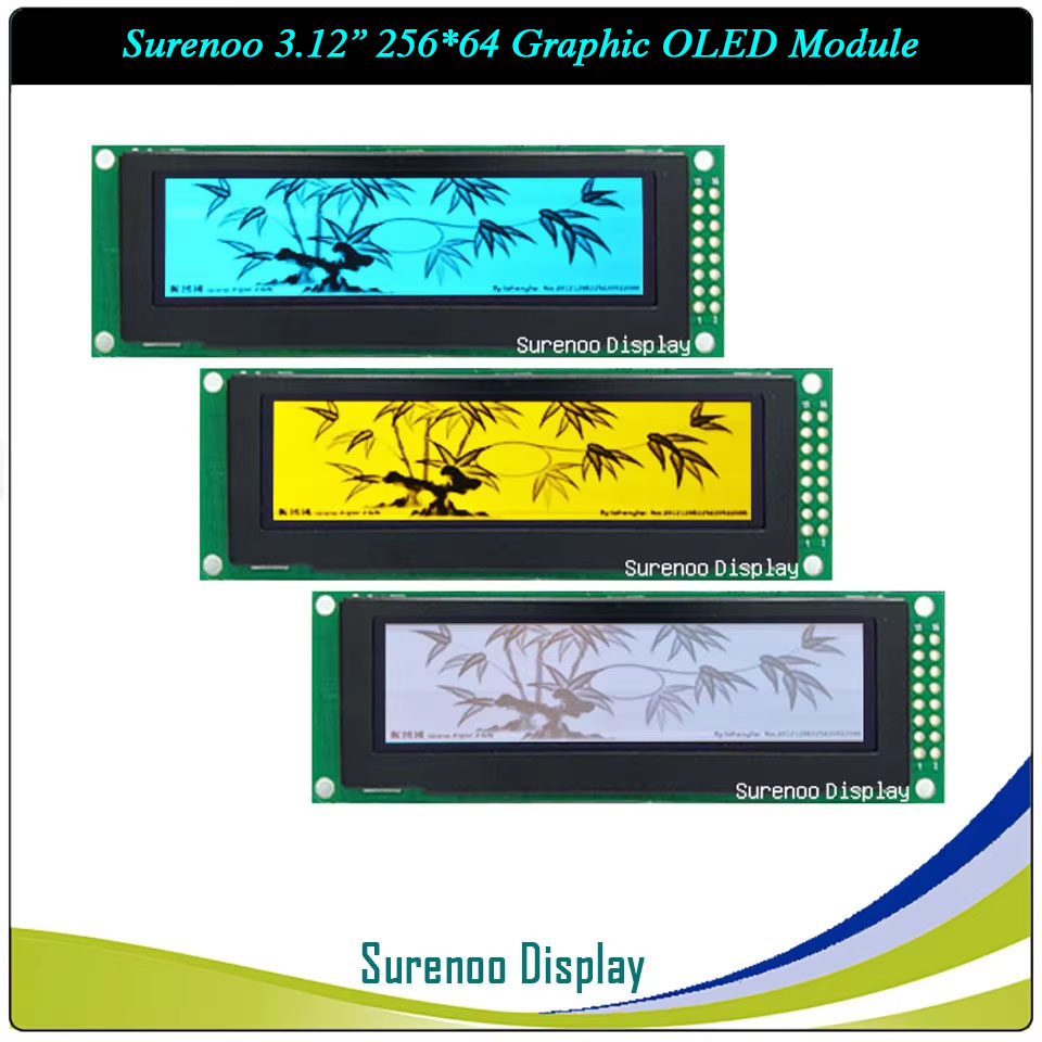
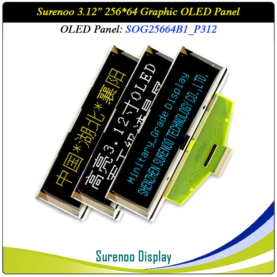
Surenoo Graphic OLED Module 3.12" 25664 256*64 256X64 Graphic LCD Module Display Screen Panel PM-OLED 6800/8080 8-Bit Parallel 3-/4- Wire Serial SPI SSD1322 Controller SOG25664B1_M312 P312
WISHLIST
Display Size: 3.12"
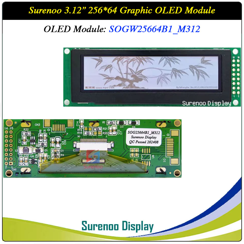
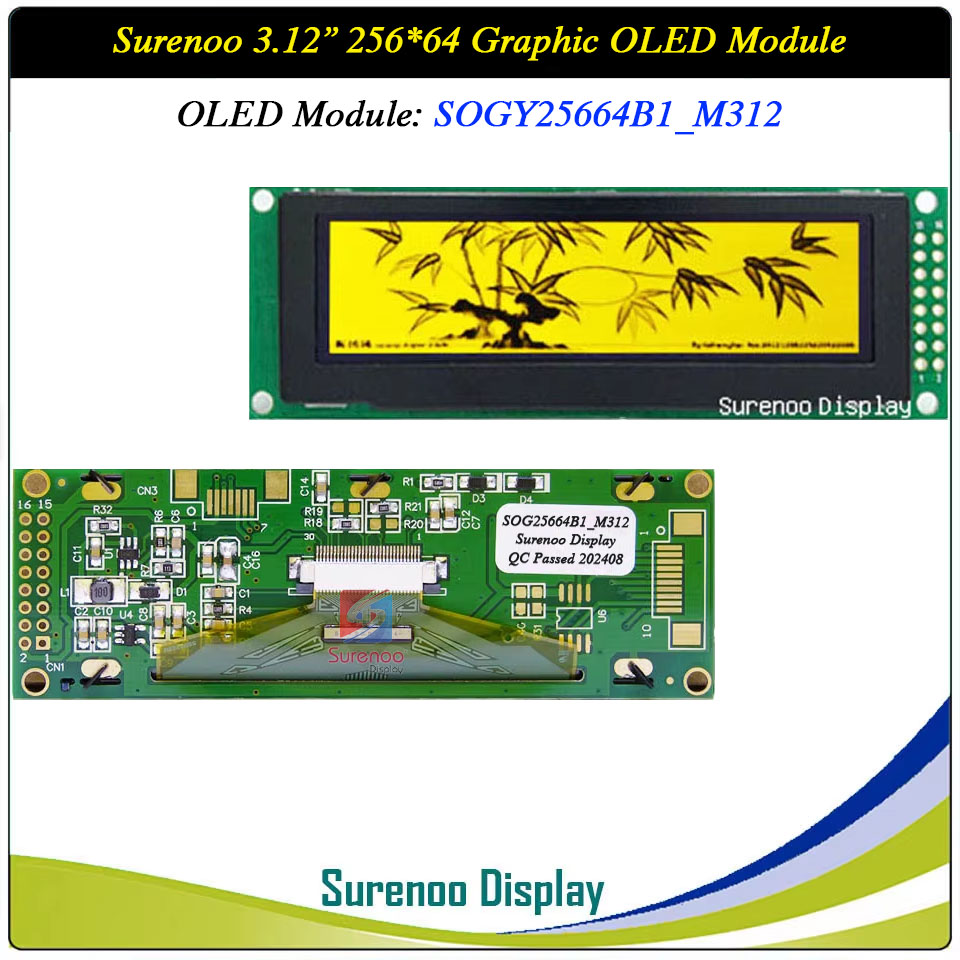
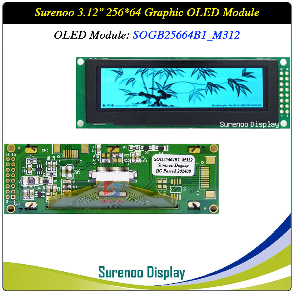
Model No.: SOG25664B1_M312
Display Format: 256*64 Dots
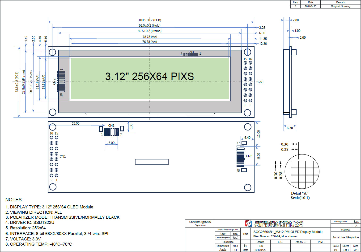
Outline: 100.50X33.50MM
Controller: SSD1322 or Equal
Model No.: SOG25664B1_M312
Display Format: 256*64 Dots
Outline: 100.50X33.50MM
Controller: SSD1322 or Equal
24 sold
Quantity
-
Detail
- Overview
It's easily controlled by MCU such as 8051, PIC, AVR, ARDUINO, ARM and Raspberry Pi. It can be used in any embedded systems, industrial device, security, medical and hand-held equipment.
- Specification
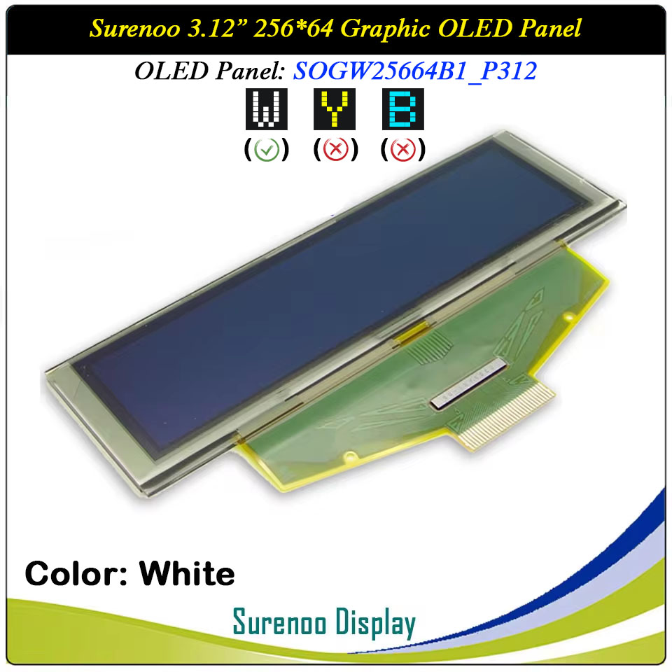
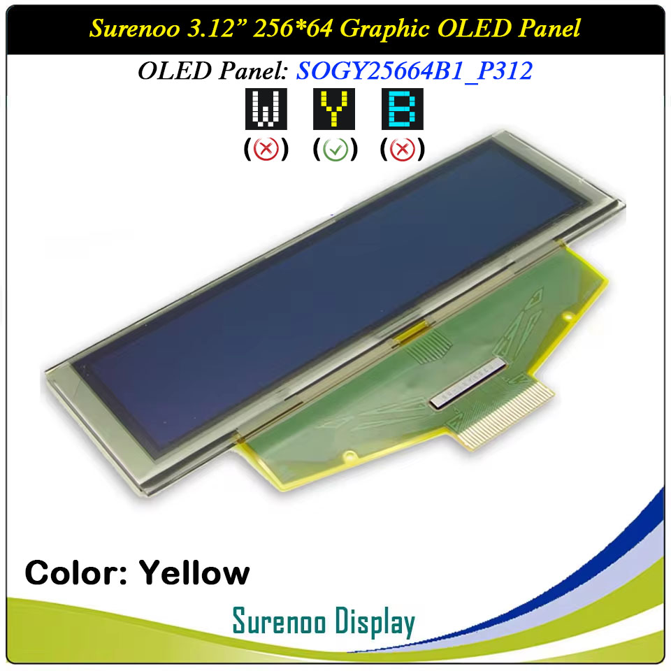
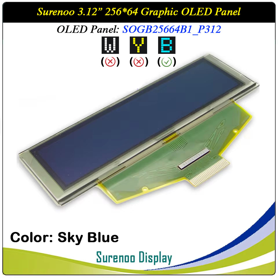
Gross Weight 0.080Kg Manufacturer Surenoo Display Type Graphic OLED Module / Graphic OLED Panel Continuity Supply More than 10 years Part No. SOG25664B1 Diagonal Size (Visual Area) 3.12" Display Format 256*64 Dots Interface 8-bit 68XX/80XX Parallel, 3-/4-wire SPI IC or Equivalent SSD1322 or Equal Voltage(Type) 3.3V Outline Dimension SOG25664B1_M312 (OLED Module), 100.50(W)x33.50(H)x6.30(T)mm SOG25664B1_P312 (OLED Panel), 88.00(W)x27.80(H)x2.00(T)mm Visual Area 78.78x21.18mm Active Area 76.78x19.18mm Dots Size 0.30x0.30mm Dots Pitch 0.28x0.28mm Display Type PM-OLED Panel Colors Code SOGW(White) / Yellow(SOGY) / Blue(SOGB) IC Package COF Viewing Direction Full Viewing Angle Operating Temperature-40℃~70℃Storage Temperature-40℃~80℃- Outline Drawing
2. OLED Panel: SOG25664B1_P312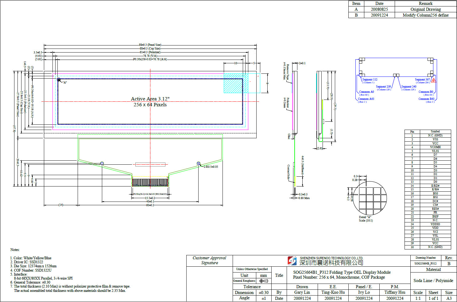
- Interface
Pin No. Pin Name Description Parallel Interface(8080): (R18, R21 USE; R19, R20 NO USE) / Parallel Interface(6800): (R18, R20 USE; R19, R21 NO USE) 1 GND Ground 0V 2 VDD Power Supply for logic (3.3V) 3 NC No connect 4-11 D0-D7 Data Bus 12 8080: RD 6800: E 8080: Active LOW Read signal 6800: Operation enable signal. Falling edge triggered. 13 8080: WR 6800: R/W 8080: Active LOW Writed signal 6800: Read/Write: R/W=1: Read; R/W:=0: Write 14 D/C (RS) H: Data; L: Command 15 /RST Active LOW Reset signal 16 /CS Chip Selection 4-SPI: (R19, R21 USE; R18, R20 NO USE) / 3-SPI: (R19, R20 USE; R18, R21 NO USE) 1 GND Ground 0V 2 VDD Power Supply for logic (3.3V) 3 NC No connect 4 SCLK (D0) Serial Clock signal 5 SDIN (D1) Serial Data Input signal 6 NC (D2) No connect 7-13 GND Ground 0V 14 4-SPI: D/C (RS) 3-SPI: GND 4-SPI: H: Data; L: Command 3-SPI: GND 15 /RST Active LOW Reset signal 16 /CS Chip Selection
1.2 OLED Module: SOG25664B1_M312 (CN2: 1X10Pin/1.0: 4-SPI)
Pin No. Pin Name Level Description 1 VDD 3.3V Power Supply for logic (3.3V) 2 NC - No Connection 3 GND 0V Ground 0V 4 SCLK H/L Serial Clock signal (OLED AND GT30L32) 5 SDIN H/L Serial Data Input signal (OLED AND GT30L32) 6 D/C H/L H: Data; L: Command (OLED Chip) 7 /RST L Active LOW Reset signal (OLED Chip) 8 /CS L Chip Selection (OLED Chip) 9 SDO H/L Serial data output (GT30L32 Font Chip) 10 /CS L Chip Selection (GT30L32 Font Chip)
1.3 OLED Module: SOG25664B1_M312 (CN2: 1X7Pin/1.0 4-SPI)
Pin No. Pin Name Level Description 1 GND 3.3V Ground 0V 2 VDD 0V Power Supply for logic (3.3V) 3 SCLK H/L Serial Clock signal (OLED Chip) 4 SDIN H/L Serial Data Input signal (OLED Chip) 5 D/C H/L H: Data; L: Command (OLED Chip) 6 /RST L Active LOW Reset signal (OLED Chip) 7 /CS L Chip Selection (OLED Chip)
2. OLED Panel: SOG25664B1_P312 (30Pin/0.5)Pin No. Symbol Type Description Power Supply 26 VCI P Power Supply for Operation
This is a voltage supply pin.
It must be connected to external source & always be equal to or higher than VDD & VDDIO.25 VDD P Power Supply for Core Logic Circuit
This is a voltage supply pin.
It can be supplied externally (within the range of 2.4~2.6V) or regulated internally from VCI. A capacitor should be connected between this pin & VSS under all circumstances.24 VDDIO P Power Supply for I/O Pin
This pin is a power supply pin of I/O buffer.
It shouldbe connected to VDD or external source. All I/O signal should have VIH reference to VDDIO. When I/O signal pins (BS0~BS1, D0~D7, control signals...) pull high, they should be connected to VDDIO.2 VSS P Ground of Logic Circuit
This is a ground pin.
It also acts as a reference for the logic pins. It must be connected to external ground.3, 29 VCC P Power Supply for OEL Panel
These are the most positive voltage supply pin of the chip.
They must be connected to external source.5, 28 VLSS P Ground of Analog Circuit
These are the analog ground pins.
They should be connected to VSS externally.Driver 22 IREF I Current Reference for Brightness Adjustment
This pin is segment current reference pin.
A resistor should be connected between this pin and VSS. Set the current lower than 10uA.4 VCOMH P Voltage Output High Level for COM Signal
This pin is the input pin for the voltage output high level for COM signals.
A tantalum capacitor should be connected between this pin and VSS.27 VSL P Voltage Output Low Level for SEG Signal
This is segment voltage reference pin.
When external VSL is not used, this pin should be left open. When external VSL is used, this pin should connect with resistor and diode to ground.Testing Pads 21 FR O Frame Frequency Triggering Signal
This pin will send out a signal that could be used to identify the driver status. Nothing should be connected to this pin. It should be left open individually.Interface 16
17BS0
BS1I Communicating Protocol SelectThese pins are MCU interface selection input. See the following table:BS0 BS1 3-wire SPI 1 0 4-wire SPI 0 0 8-bit 68XX Parallel 1 1 8-bit 80XX Parallel 0 1 20 RES# I Power Reset for Controlle and Driver
This pin is reset signal input.
When the pin is low, initialization of the chip is executed.19 CS# I Chip Select
This pin is the chip select input.
The chip is enabled for MCU communication only when CS# is pulled low.18 D/C# I Data/Command Control
This pin is Data/Command control pin.
When the pin is pulled high, the input at D7~D0 is treated as display data.When the pin is pulled low, the input at D7~D0 will be transferred to the command register. For detail relationship to MCU interface signals, please refer to the Timing Characteristics Diagrams.14 E/RD# I Read/Write Enable or Read
This pin is MCU interface input.
When interfacing to a 68XX-series microprocessor, this pin will be used as the Enable (E) signal. Read/write operation is initiated when this pin is pulled high and the CS# is pulled low.When connecting to an 80XX-microprocessor, this pin receives the Read (RD#) signal. Data read operation is initiated when this pin is pulled low and CS# is pulled low.When serial mode is selected, this pin must be connected to VSS.15 R/W# I Read/Write Select or Write
This pin is MCU interface input.
When interfacing to a 68XX-series microprocessor, this pin will be used as Read/Write (R/W#) selection input. Pull this pin to “High’ for read mode and pull it to“ow, for write mode.When 80XX interface mode is selected, this pin will be the Write (WR#) input. Data write operation is initiated when this pin is pulled low and the CS# is pulled low.When serial mode is selected, this pin must be connected to VSS.6~13 D7-D0 I/O Host Data Input/Output Bus
These pins are 8-bit bi-directional data bus to be connected to the microprocessor mode is selected, D1 will be the serial data input SDIN and D0 will be the serial clock input SCLK. Unused pins must be connected to VSS except for D2 in serial mode.Reserve 23 NC - Reserved Pin
The NC pin between function pins are reserved for compatible and flexible design.1, 30 NC (GND) - Reserved Pin (Supporting Pin)
The supporting pins can reduce the influences from stresses on the function pins. These pins must be connected to external ground.Please download the datasheet to get the detailed Pin description.- Documents
No. Item File Name File Type ICON Date Description Mark 1 Datasheet SOG25664B1_M312 PDF 
2013-03-17 Standard 256*64 Graphic OLED Module SOG25664B1_P312 PDF 2013-03-17 Standard 256*64 Graphic OLED Panel 2 Controller SSD1322 PDF 2008-09-24 SSD1322 is a COG Graphic 256*64 OLED Controller -
Customer ReviewsNo comments